The Doc whom IoT Professionals trust

Autor: Dr. Mountain

Tech Guide: Google Cloud IoT Architecture

Reading Time: 4 Minutes

Data pipeline to visualize data from an IoT device based on standard services of the Google Cloud Platform

Key prerequisite:

  • Data-driven
  • Free of charge
  • Cloud first, only

After Microsoft Azure and Amazon Web Services (AWS), the Google Cloud Platform (GCP) was the third-most used Public Cloud provider in the year 2021.[1] Just like the other Cloud providers, it offers multiple products as-a-Service (aaS) related to Infrastructure aaS, Platform aaS, or Software aaS (cf. Google Cloud products). There is also the typical Cloud trap of „20+ free products“ as well as of „$300 in free credits[2], aiming for a vendor lock-in on client-side. Google even provides a detailed comparison of its own service offerings to the other two big players in the Cloud game: Azure and AWS

The Scope

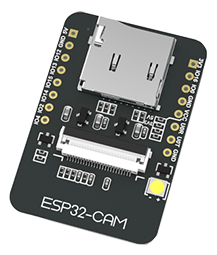
Based on the variety of Cloud services offered and the Cloud trap of free products, we are implementing a data pipeline for a typical use case in the scope of the Internet of Things (IoT). The cloud-native pipeline should collect and visualize data of an IoT device like the famous ESP32 based on Cloud services. More precisely, the pipeline streams the data from the source to a dashboard, including the processing and storing of the data in the Cloud. As key prerequisite of the cloud-native pipeline related to IoT data, we define the following three measures:

  • Data-driven: End-to-end pipeline for data from source to user
  • Free of charge: No fees for using the services offered in GCP
  • Cloud first, Cloud only: Only Cloud services used, no services on-site

Luckily, we are fulfilling all three as you find out next.

The Pipeline

The following figure shows the different stages of the data pipeline, starting at the source till the visualization of the data. Furthermore, it also highlights the corresponding services used of the Google Cloud Platform in each stage:

Data Pipeline from a Data Source (e.g., an ESP32) to Data Access
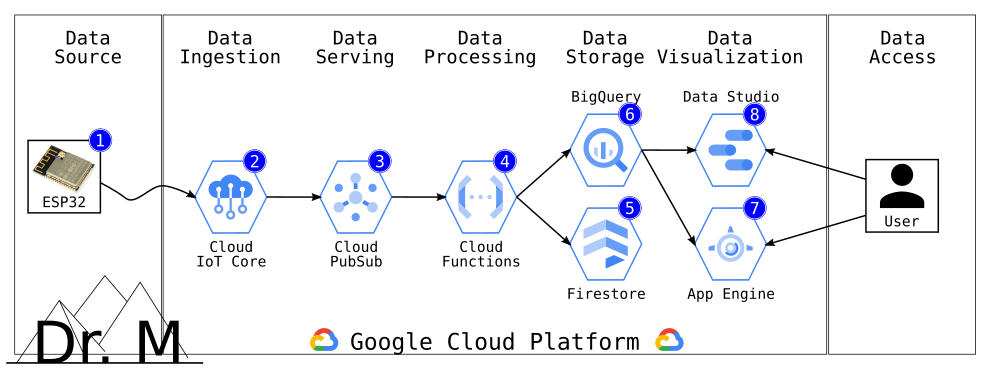
based on Services of the Google Cloud Platform

The overall pipeline includes seven stages, why we split this technical guide into seven posts along the different stages:

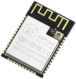
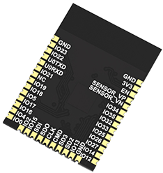
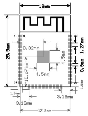
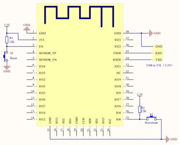
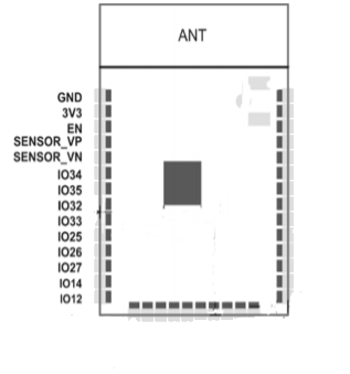
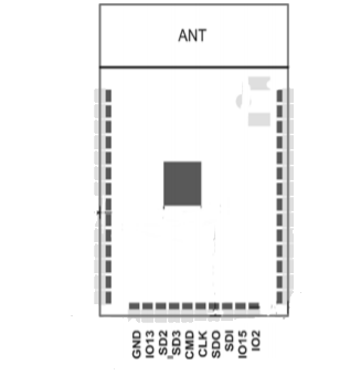
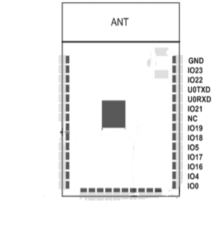
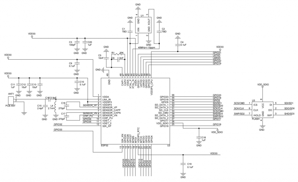
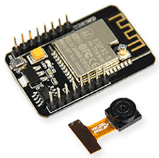
  • The 1st stage is about the Data Source, focusing on the IoT device like monitoring the environment, structuring the information monitored, and sending the structured information to the Cloud. For more information about the first stage, visit the related blog post.
    <Stay tuned, blog and link follow soon>
  • The 2nd stage is about the Data Ingestion, focusing on the service Cloud IoT Core. It is a message broker — more precisely, an MQTT broker — with additional functionality like a device registry. For more information about the first stage, visit the related blog post.
    <Stay tuned, blog and link follow soon>
  • The 3rd stage is about the Data Serving, focusing on the service Cloud PubSub. It offers to ingest events for streaming into data lakes or databases. For more information about the first stage, visit the related blog post.
    <Stay tuned, blog and link follow soon>
  • The 4th stage is about the Data Processing, focusing on the service Cloud Functions. It offers Serverless Computing, also known as Function as a Service (FaaS), for a variety of programming languages. For more information about the first stage, visit the related blog post.
    <Stay tuned, blog and link follow soon>
  • The 5th stage is about the Data Storage, focusing on the services BigQuery and Firestore. BigQuery offers a serverless, highly scalable, and cost-effective data warehouse. Firestore offers a flexible, fully managed, and scalable NoSQL database (document database). For more information about the first stage, visit the related blog post.
    <Stay tuned, blog and link follow soon>
  • The 6th stage is about the Data Visualization, focusing on the services Data Studio and App Engine. Data Studio offers interactive dashboards and beautiful reports. App Engine offers highly scalable applications on a fully managed serverless platform. For more information about the first stage, visit the related blog post.
    <Stay tuned, blog and link follow soon>
  • Last, the 7th stage is about the Data Access, focusing on the service Identity-aware Proxy (IAP). It offers the usage of identity and context to guard access to Internet-facing applications. For more information about the first stage, visit the related blog post.
    <Stay tuned, blog and link follow soon>

The Summary

The Cloud enables the change from CapEx (Capital Expenditures) to OpEx (Operational Expenditure) by shifting investments for the on-premise infrastructure to payments for the usage of managed services at the Cloud. Based on the managed services offered of the Google Cloud Platform (GCP), we build a cloud-native pipeline for data related to an IoT use case. The data pipeline includes seven stages, ranging from the data source like an IoT device to the data access like user identity. Furthermore, we define the following key prerequisite to be fulfilled: Data-driven, free of charge, and Cloud first, only. And, as you can read in the separate blog posts for each stage, we nailed! We build an end-to-end pipeline for IoT data that totally uses managed services in the Cloud — more precisely, the GCP — without any fees charged.

References

  1. Worldwide Market Share of Service Providers for Cloud Infrastructure from the 4th quarter 2017 to the 3rd quarter 2021 [last checked 2021-11-15]
  2. Google Cloud Free Programm [last checked 2022-02-09]

Eclipse Unide: A Simple Payload Specification

Reading Time: 2 Minutes

Leveraging the Eclipse IoT stack for scenarios in the Industry 4.0

Eclipse Unide

Release of Version 3 of the PPMP

The Eclipse Unide project extends the existing Eclipse IoT world about a simple information structure, called Production Performance Management Protocol (PPMP). Besides the publication of the current version of PPMP, it also develops simple Client-Server implementations (cf. GitHub).

The PPMP defines an easy and lightweight format to gather the necessary information from sensors or machines like time-series data. The format specifies a JSON (JavaScript Object Notation) payload, flexible enough to be transferred via a variety of protocols like HTTPS, AMQP or MQTT. In detail, the specification of the JSON payload includes three types of messages:

To validate a related payload of the PPMP, just enter the reference

https://raw.githubusercontent.com/eclipse/unide/master/ppmp/ppmp-schema/src/main/resources/org/eclipse/iot/unide/ppmp/v3/process_schema.json

as schema and the payload in, for instance, the JSON Schema validator. The structure of the payload is easily understandable and very lightweight. For instance, the following JSON payload is a minimal message of a machine:

{
   "content-spec": "urn:spec://eclipse.org/unide/machine-message#v3",
   "device": {
      "id": "a4927dad-58d4-4580-b460-79cefd56775b"
   },
   "messages": [
      {
         "ts": "2022-02-04T18:14:07.827Z",
         "code": "190ABT"
      }
   ]
}

and of a measurement:

{
   "content-spec": "urn:spec://eclipse.org/unide/measurement-message#v3",
   "device": {
      "id": "a4927dad-58d4-4580-b460-79cefd56775b"
   },
   "measurements":
      {
         "ts": "2022-02-04T18:14:01.382Z",
         "series": {
            "time":
               0,
               21,
               42
            ],
            "temperature":
               45.4231,
               46.4222,
               44.2432
            ]
         }
      }
   ]
}

The primary goal of the protocol design is to gather and aggregate data of different devices like machines or sensors. To ensure interoperability between different types of devices and software, the protocol includes mandatory and optional fields of data and related metadata.

A closer look on the list of interested parties offers key players like Bosch Software Innovations GmbH or SAP.

Reading Time: 2 Minutes


The data sheet of the ESP32 states its electrical characteristics (cf. esp32_datasheet_en.pdf). It specifies the absolute maximum ratings and the recommended ratings of the supply voltage applied to the power supply pins (cf. Conclusion).

Absolute Maximum Ratings

The absolute maximum rating of the voltage applied to the power supply pins VDDA, VDD3P3_RTC, VDD3P3, VDD3P3_CPU, and VDD_SDIO is between a minimum voltage of -0.3 volts and a maximum voltage of 3.6 volts. Please note that a voltage below or above the absolute maximum rating may cause a permanent damage to the ESP32 chip.

SymbolParameterMinMaxUnit
VDDA, VDD3P3_RTC, VDD3P3, VDD3P3_CPU,
and VDD_SDIO
Voltage applied to power supply pins-0.33.6V
Espressif ESP32 Data Sheet (cf. Table 11)

The recommended rating of the voltage applied to the power supply pins VDDA, VDD3P3_RTC, VDD3P3, and VDD_SDIO depends on the presence of a 3.3V flash embedded (cf. Ordering Information):

  • The ESP32 chip with the ordering code ESP32-U4WDH has a 4 MB embedded flash (80 MHz). As a result, the applied voltage is between a minimum voltage of 3.0 volts and a maximum voltage of 3.6 volts with a typical voltage of 3.3 volts.
  • The ESP32 chips with the ordering codes ESP32-D0WD-V3, ESP32-D0WDQ6-V3, ESP32-D0WD, ESP32-D0WDQ6, and ESP32-S0WD have no embedded flash. As a result, the applied voltage is between a minimum voltage of 2.3 volts and a maximum voltage of 3.6 volts with a typical voltage of 3.3 volts.

Be aware in both cases that writing to eFuse, the voltage applied to the power supply pin VDD3P3_RTC should be at least 3.3 volts.

The recommended rating of the voltage applied to the power supply pin VDD3P3_CPU is between a minimum voltage of 1.8 volts and a maximum voltage of 3.6 volts with a typical voltage of 3.3 volts.

SymbolParameterMinTypMaxUnit
VDDA, VDD3P3_RTC, VDD3P3, and VDD_SDIOVoltage applied to power supply pins2.3 / 3.03.33.6V
VDD3P3_CPUVoltage applied to power supply pin1.83.33.6V
Espressif ESP32 Data Sheet (cf. Table 12)

Conclusion

The operating voltage applied to the power supply pins ranges from 1.8 / 2.3 / 3.0 volts to 3.6 volts, where the recommended voltage of the power supply is 3.3 volts. Moreover, the recommended current delivered by external power supply 500 milliampere (or even more).


Release Notes:

  • [2021-09-04] Initial release of the blog post comprising the specifications of the absolute maximum ratings and the recommended ratings of the supply voltage applied to the power supply pins.

Technical Deep-dive into Voltage Divider based on Resistors

Reading Time: 4 Minutes

This blog post gives a deeper understanding of a voltage divider, more precisely a resistive voltage divider. Based on two resistors connected in series, typical use cases are the creation of a reference voltage or a voltage reduction to measure it.

Table of Content

First, the blog post explains a generic voltage divider (cf. Introduction), followed by the description of a resistive divider (cf. Resistor-based Voltage Divider). Based on the described equation of a resistive divider, the blog post calculates an output voltage (cf. Exemplary Calculation) and proofs the stated equation of a resistive divider (cf. Proof of Equation). Afterwards, the blog post explains a resistive divider under load (cf. Behavior Under Load) and finally concludes (cf. Conclusion).


Introduction

A voltage divider is a passive linear circuit. It consists of two passive components, connected in series. Due to the connection in series of the two components, the output voltage is a fraction of the input voltage. The division of the input voltage results from its distribution among the two components. Depending on the use case, the two components are typically any combination of resistors, inductors, and capacitors. Most common, the two components are resistors, resulting in a resistive divider. Also common as a voltage divider are the combination of a resistor and a capacitor (low-pass RC filter), two inductors (inductive divider), or two capacitors (capacitive divider).

Resistor-based Voltage Divider

The typical voltage divider is a circuit with two resistors, connected in series. A common use case of such a resistive divider is the creation of a reference voltage or the reduction of the input voltage for measurements. The created output voltage depends upon the existence of a load (cf. Behavior Under Load) or the non-existence of a load, named open circuit behavior, explained below:

Resistor-based Voltage Divider:
Open Circuit Behavior

Knowing the resistance R1 and R2 of the two resistors, the output voltage V2 is:

(1)    \begin{equation*}  V_2 = \frac{R_2}{(R_1 + R_2)} * V_{Total} \end{equation*}

and, likewise, for the output voltage V1:

(2)    \begin{equation*}  V_1 = \frac{R_1}{(R_1 + R_2)} * V_{Total} \end{equation*}

Exemplary Calculation

The following figure shows an exemplary voltage divider based on two resistors, connected in series:

An Exemplary Voltage Divider based on Two Resistors Connected in Series

The resistance of the four-band resistor R1 is 1k Ohms with a tolerance of ±1% and the resistance of the four-band resistor R2 is 5k Ohms with a tolerance of ±1%. For instance, use the following calculator for the color code of resistors:

Moreover, the battery-based power supply delivers an input voltage of 8.4 volts (VTotal) due to two fully-charged LiPo batteries (read more about a LiPo-based power supply for the ESP32-CAM here). Now, let’s calculate the output voltage:

(3)    \begin{equation*} \begin{split} V_2 &= \frac{R_2}{(R_1 + R_2)} * V_{Total} \\ &= \frac{5000}{1000 + 5000} * 8.4 \\ &= \frac{5}{6} * 8.4 = 7 \end{split} \end{equation*}

Proof of Equation

To proof Equation (1) stated above, let’s start with Ohm’s Law, and especially for the second resistor R2:

(4)    \begin{equation*}  \begin{split} V &= R * I \\ &\Rightarrow V_2 = R_2 * I_2 \end{split} \end{equation*}

Based on the series connection of the resistors, the current flowing through the circuit is constant (I = ITotal = I1 = I2) and the total overall resistance of the circuit is RTotal = R1 + R2 (cf. behavior of series circuits):

(5)    \begin{equation*}  \begin{split} V_2 &= R_2 * I_2 = R_2 * I \\ &\Rightarrow I = \frac{V_2}{R_2} \end{split} \end{equation*}

(6)    \begin{equation*}  \begin{split} V_{Total} = R_{Total} * I_{Total} = (R_1 + R_2) * I \end{split} \end{equation*}

Now, let’s combine Equation (3) and Equation (4):

(7)    \begin{equation*}  \begin{split} V_{Total} &= (R_1 + R_2) * I \\ & = (R_1 + R_2) * \frac{V_2}{R_2} \\ & \Rightarrow V_2 = R_2 * \frac{V_{Total}}{(R_1 + R_2)} \end{split} \end{equation*}

That’s it, QED!

Behavior Under Load

In case the output voltage V2 depends upon the existence of a load RL, the circuit of a resistive divider changes from a series connection to a series and parallel connection. The load adds to the two resistors R1 and R2 another resistance RL, connected in parallel to the resistance R2 (R2 || RL). Thus, the series connection under load extends to R1 + (R2 || RL):

Resistor-based Voltage Divider:
Behavior Under Load

Due to the load added, the total overall resistance RTotal of the circuit decreases:

(8)    \begin{equation*} \begin{split} R_{Total} &= R_1 + \frac{1}{\frac{1}{R_2} + \frac{1}{R_L}} \\ &= R_1 + \frac{R_2 * R_L}{R_2 + R_L} \end{split} \end{equation*}

and the total overall current ITotal flowing through the circuit increases:

(9)    \begin{equation*} I_{Total} = I_2 + I_L \end{equation*}

resulting in an increase of the voltage V1 and a decrease of the voltage V2 . To calculate the output voltage V2 of a resistive voltage divider under load, we first define a forward slope resistance R2L and set it in Equation (1):

(10)    \begin{equation*} R_{2L} = R_2 || R_L = \frac{R_2 * R_L}{R_2 + R_L} \end{equation*}

(11)    \begin{equation*} V_2 = \frac{R_{2L}}{R_1 + R_{2L}} * V_{Total} \end{equation*}

In order that the load RL has as less effect as possible on the output voltage V2, the resistance R1 and R2 should be considerably smaller than the load RL:

(12)    \begin{equation*}  \begin{split} R_i &= R_1 || R_2 = \frac{1}{\frac{1}{R_1} + \frac{1}{R_2}} = \frac{R_1 * R_2}{R_1 + R_2} \\ R_i &\ll R_L \Rightarrow R_i < \frac{1}{10} * R_L \end{split} \end{equation*}

Conclusion

A resistive voltage divider is a passive linear circuit, consisting of two resistors connected in series. Due to the distribution of the input voltage among the two resistors (series connection), the output voltage is a fraction of the input voltage:

(13)    \begin{equation*}  V_2 = \frac{R_2}{(R_1 + R_2)} * V_{Total} \end{equation*}


Release Notes:

  • [2021-08-19] Initial release of the blog post comprising the description of the resistor-based voltage divider without a load (open circuit behavior), an exemplary calculation of an output voltage, and the proof of the equation
  • [2021-09-11] Update of the blog post adding the description of the resistor-based voltage divider under load (behavior under load)

Power up the ESP32-CAM on the Input Voltage Pin 5V

Reading Time: 2 Minutes

This blog post explains the easiest way of powering up the ESP32-CAM board: Connecting an external power supply to the input voltage pin 5V on the board.

On the ESP32-CAM board, the soldered voltage regulator AMS1117-3.3 (read more about the AMS1117-3.3 here) regulates the voltage connected on the input voltage pin 5V. It delivers an output voltage of 3.3 volts and a maximum current of 1.5 amperes. To this end, the voltage regulator requires an input voltage greater than 4.5 volts due to a dropout voltage of 1 volt. In detail, both a laboratory power supply or a battery-based power supply can deliver the required input voltage.

Laboratory Power Supply

The function of a laboratory power supply is to supply a constant voltage (typically indicated by „C.V.“) or a constant current (typically indicated by „C.C.“). It converts an unregulated alternating current (AC) into a constant direct current (DC). Usually, a laboratory power supply delivers a variety of continuous or preset voltages (read more about regulated power supply on Wikipedia).

Now, it is time to power up the ESP32-CAM board with a laboratory power supply that delivers the constant voltage required:

  1. Set the output voltage of the laboratory power supply to a fixed voltage between 5 volts and 6 volts
  2. Connect the output voltage of the power supply to a ground pin GND and the input voltage pin 5V
  3. Turn on the voltage supply of the laboratory power supply to provide the required input voltage of greater than 4.5 volts to the AMS1117-3.3

That’s it. The external power supply together with the AMS1117-3.3 power up the ESP32-CAM board.

Battery-based Power Supply

A battery-based power supply delivers an output voltage, depending on the type of the battery. For instance, a Lithium-Ion Polymer (LiPo) battery delivers an output voltage of 4.2 volt, if it is fully-charged. While discharging, the supplied output voltage decreases to 3.7 volts. Please note that the output voltage of a LiPo battery should not reach 2.5 volts or less – better 3 volts or less. Otherwise, it could permanently damage the LiPo battery:

Typical Voltage Discharging Curve of a Lithium-Ion Polymer Battery

Due to the required input voltage of greater than 4.5 volts, the number of needed LiPo batteries is two LiPo batteries connected in series:

Battery-based Power Supply by 2 LiPos of ESP32-CAM board

In detail, two fully-charged LiPo batteries connected in series supply an output voltage of 8.4 volts to the AMS1117-3.3, powering up the ESP32-CAM board. While discharging, the two LiPo batteries supply an output voltage of 7.4 volts, decreasing to an output voltage of 5 volts. To prevent the two LiPo batteries from a permanently damage, completely disconnect the two LiPo batteries from the electrical circuit, latest reaching the critical low voltage of 5 volts – better 6 volts.

Technical Deep-Dive into Linear Voltage Regulator

Reading Time: 2 Minutes

This blog post gives a deeper understanding of a linear voltage regulator. A (linear) voltage regulator plays an important role as power supply. Its main function is to automatically output a constant voltage by adjusting continuously a voltage divider network. Thus, it acts as a variable resistor, where the resistance of the regulator depends on both the input voltage and the load (cf. Ohm’s law). The voltage U in units of volts equals to the resistance R in units of ohms multiplied by the current I in units of amperes:

U = R * I

To drop some voltage on the variable resistance, the input voltage VIN of the regulator must be higher than the regulated output voltage VOUT. This difference between the input voltage and the regulated output voltage (VIN - VOUT) is called dropout voltage. The regulator has to dissipate the power loss – more precisely, the multiplication of the dropout voltage and the current drawn by the circuit – as heat. Due to the waste of energy as heat regulating the voltage, a linear voltage regulator has a limited efficiency. The heat dissipated by the regulator relates directly to the average amount of electric power dissipated by the regulator. The electric power P in units of watts equals to the voltage U in units of volts multiplied by the current I in units of amperes:

P = U * I = (VIN - VOUT) * IMAX

where VIN is the input voltage of the regulator, VOUT the regulated output voltage of the regulator powering the circuit, and IMAX the maximum current drawn by the circuit. For a safe estimation, the equation calculates the peak power with the maximum current drawn (worst-case scenario), not continuously draw by the circuit. Thus, the regulator has to dissipate more heat (power loss) as, on the one hand, the difference of the input voltage and the regulated output voltage gets greater, and/or, on the other hand, the current drawn gets greater. To expose more heat from a regulator under load, a heat sink with „fins“ increases the surface area of the regulator, cooling it more efficiently.

The figure below shows an exemplary circuit of a constant power supply of 9 volts (input voltage), a fixed voltage regulator producing a fixed DC output voltage of 3.3 volts, and an external device drawing 0.25 ampere:

Exemplary circuit of a constant power supply, a fixed voltage regulator, and an external device.

Based on the three input parameters VIN, VOUT, and IMAX, the regulator has to dissipate a peak power of 1.425 watts: (9V - 3.3V) * 0.25A

Power up the ESP32-CAM

Reading Time: 3 Minutes

Now, it is time to power the ESP32-CAM board and get the hands-on it. This blog post gives an understanding of the possible power supplies of the board. In total, the board has two different options for power supply: Either an unregulated power to the ground pin GND and the input voltage pin 5V or a regulated power to the ground pin GND and the input voltage pin 3V3. Or jump directly to the conclusion.

ESP32-CAM: Front-View
ESP32-CAM: Back-View

First Option: Connecting an external unregulated power supply (up to 15 Volt) to the ground pin and the input voltage pin 5 Volt

The ESP32-CAM board has a linear, Low-DropOut (LDO) voltage regulator – more precisely, the AMS1117-3.3 (read more about the AMS1117-3.3 here). It provides an output voltage of 3.3 Volt by a maximum output current of 1.5 Ampere and a maximum input voltage of 15 Volt. At the maximum output current of 1.5 Ampere, the ASM1117-3.3 operates with a dropout voltage (input-to-output differential) of 1.3 Volt, decreasing down to 1 Volt at lower load currents. The output voltage of 3.3 Volt powers the different components on the ESP32-CAM like the camera, the Pseudo-Random Access Memory (PSRAM), or the Micro SD-Card:

ESP32-CAM: Schematic Diagram of the External Power Supply (source)

Due to the soldered AMS1117-3.3, the ESP32-CAM board supports on the input voltage pin 5V an external unregulated power supply between 4.5 Volt (output voltage + dropout voltage) and up to a maximum of 15 Volt. Any voltage higher than 4.5 Volt, the AMS1117-3.3 has to dissipate the excessive voltage – more precisely, the power that equals to (VIN - VOUT) * Aas heat on the voltage regulator (read more about linear voltage regulators here). So, it is best to keep the input voltage close to 5 Volt, avoiding too much loss of power as heat on the voltage regulator (not heat dissipation mounted).

Second option: Connecting an external regulated power supply of 3.3 Volt to the ground pin and the input voltage pin 3V3

The ESP32-CAM board supports the power supply by an external regulated power of 3.3 Volt, connected to the ground pin GND and the input voltage pin 3V3 (cf. front-view and back-view of ESP32-CAM). As shown above in the schematic diagram, the power supply 3V3 bypasses the on-board voltage regulator AMS1117-3.3. As a result, the ESP32-CAM board has no protection against over-voltage, damaging the soldered components on the board. Be very careful that the connected input voltage on pin 3V3 is safe and regulated between 3 Volt and 3.6 Volt (recommended operating voltage of the ESP32 is 3.3 Volt).

Conclusion

To power the ESP32-CAM board, there are two options available:

First, an external unregulated voltage between 4.5 Volt and 15 Volt connected to the ground pin GND and the input voltage pin 5V. The ESP32-CAM board regulates the supplied input voltage on-board with the soldered AMS1117-3.3 to the required input voltage of 3.3 Volt.

Second, an external regulated voltage of 3.3 Volt connected to the ground pin GND and the input voltage pin 3V3. Be careful that the supplied voltage is not higher than 3.6 Volt! Exceeding the voltage limit will cause damages of the ESP32-CAM board.

Please note that the ESP32-CAM board should only be powered by the first option (unregulated) or the second option (regulated), NEVER EVER1 at the same time! Otherwise, both power supplies at the same time will surely damage the ESP32-CAM board.


Footnote

1. Thanks to the feedback from Doug (cf. comments)

AMS1117-3.3: The Linear Voltage Regulator on the ESP32-CAM

Reading Time: 2 Minutes

The ESP32-CAM uses the fixed, linear voltage regulator AMS1117-3.3 from Advanced Monolithic Systems (AMS) that possesses a built-in protection against short circuit and thermal overloads:

ESP32-CAM w/ ASM1117 highlighted
AMS1117 SOT-223 Top View

For instance, the circuitry-wise thermal protection will shut-down the linear regulator in case the junction temperature is above 165 °C at the sense point. It provides an output voltage of 3.3V by a maximum output current of 1.5A and a maximum input voltage of 15V. The AMS1117-3.3 guarantees a low dropout voltage (input-to-output differential: VDROPOUT = VIN – VOUT) of maximum 1.3V at the maximum output current of 1.5A. The dropout voltage decreases at lower load currents and operates down to 1V dropout voltage. The on-chip trimming develops a reference voltage of 1.25V between the output and the ground with a precise reference tolerance of 1.5%.

Electrical Characteristics

The table below shows the electrical characteristics of the AMS1117-3.3 at IOUT = 0 mA, and TJ = +25°C (unless specified otherwise):

ParameterConditionsMinTypMaxUnits
Reference VoltageIOUT = 10 mA
1.5 V ≤ (VIN – VOUT) ≤ 12 V
1.21251.2501.2875V
Output VoltageVIN = 4.8V3.2013.3003.399V
Line Regulation1.5V ≤ (VIN – VOUT) ≤ 12V1.010mV
Load RegulationVIN = 4.75V, 0 ≤ IOUT ≤ 0.8A725mV
Dropout Voltage∆VOUT, ∆VREF = 1%, IOUT = 0.8A1.11.3V
Current Limit(VIN – VOUT) = 1.5V90011001500mA
Minimum Load
Current
(VIN – VOUT) = 1.5V510mA
Quiescent Current(VIN – VOUT) = 1.5V511mA
Cf. data sheet of the AMS1117

Deep Dive on the ESP32-S from Ai-Thinker

Reading Time: 3 Minutes

The ESP32-S from Ai-Thinker is a small-size, low-power wireless module for a wide variety of applications like a low-power sensor with a demanding task such as voice encoding. It is based on the famous ESP32 from Espressif, more precisely the ESP32-D0WDQ6 chip, designed to be scalable and adaptive. Please have a look at the following post for an in-detail description of the related features and specifications of the ESP32 chip (coming soon). The ESP32-S is Ai-Thinker’s equivalent to the ESP32-WROOM-32 module from Espressif, equaling in the form factor and specifications.

ESP32-S Front-View
Front View (Source)
ESP32-S Back View
Back View (Source)

Pin Definitions

ESP32-S Pin Layout
ESP32-S Pin-Out

The ESP32-S has a length of 18 mm, a width of 25.5 mm and a height of 2.8 mm ∓ 0.1 mm. Furthermore, it has 38 pins, defined as follows (cf. Datasheet):

The following table shows the name, type, number and function of the pins on the left-side of the ESP32-S:

ESP32-S Pin-Out
NameTypeGPIOFunction
GNDPGround
3V3PPower Supply: 3.3V (VDD), 500 mA
ENIChip-enable Signal (Active high)
SENSOR_VPIADC_H, ADC1_CH0, RTC_GPIO0
SENSOR_VNIADC1_CH3, ADC_H, RTC_GPIO3
IO34IGPIO34ADC1_CH6, RTC_GPIO4
IO35IGPIO35ADC1_CH7, RTC_GPIO5
IO32I/OGPIO32XTAL_32K_P (32.768kHz crystal oscillator input), ADC1_CH4, TOUCH9, RTC_GPIO9
IO33I/OGPIO33XTAL_32K_N (32.768kHz crystal oscillator output), ADC1_CH5, TOUCH8, RTC_GPIO8
IO25I/OGPIO25DAC_1, ADC2_CH8, RTC_GPIO6, EMAC_RXD0
IO26I/OGPIO26DAC_2, ADC2_CH9, RTC_GPIO7, EMAC_RXD1
IO27I/OGPIO27ADC2_CH7, TOUCH7, RTC_GPIO17, EMAC_RX_DV
IO14I/OGPIO14ADC2_CH6, TOUCH6, RTC_GPIO16, MTMS, HSPICLK, HS2_CLK, SD_CLK, EMAC_TXD2
IO12I/OGPIO12ADC2_CH5, TOUCH5, RTC_GPIO15, MTDI, HSPIQ, HS2_DATA2, SD_DATA2, EMAC_TXD3
Mapping of the pins at the left-side of the ESP32-S

The following table shows the name, type, number and function of the pins on the bottom of the ESP32-S:

ESP32-S Pin-Out
NameTypeGPIOFunction
GNDPGround
IO13I/OGPIO13ADC2_CH4, TOUCH4, RTC_GPIO14, MTCK, HSPID, HS2_DATA3, SD_DATA3, EMAC_RX_ER
SHD/SD2I/OGPIO9SD_DATA2, SPIHD, HS1_DATA2, U1RXD
SWP/SD3I/OGPIO10SD_DATA3, SPIWP, HS1_DATA3, U1TXD
SCS/CMDI/OGPIO11SD_CMD, SPICS0, HS1_CMD, U1RTS
SCK/CLKI/OGPIO6SD_CLK, SPICLK, HS1_CLK, U1CTS
SDO/SD0I/OGPIO7SD_DATA0, SPIQ, HS1_DATA0, U2RTS
SDI/SD1I/OGPIO8SD_DATA1, SPID, HS1_DATA1, U2CTS
IO15I/OGPIO15ADC2_CH3, TOUCH3, MTDO, HSPICS0, RTC_GPIO13, HS2_CMD, SD_CMD, EMAC_RXD3
IO2I/OGPIO2ADC2_CH2, TOUCH2, RTC_GPIO12, HSPIWP, HS2_DATA0, SD_DATA0
Mapping of the pins at the botom of the ESP32-S

The following table shows the name, type, number and function of the pins on the right-side of the ESP32-S:

ESP32-S Pin-Out
NameTypeGPIOFunction
IO0I/OGPIO0ADC2_CH1, TOUCH1, RTC_GPIO11, CLK_OUT1, EMAC_TX_CLK
IO4I/OGPIO4ADC2_CH0, TOUCH0, RTC_GPIO10, HSPIHD, HS2_DATA1, SD_DATA1, EMAC_TX_ER
IO16I/OGPIO16HS1_DATA4, U2RXD, EMAC_CLK_OUT
IO17I/OGPIO17HS1_DATA5, U2TXD, EMAC_CLK_OUT_180
IO5I/OGPIO5VSPICS0, HS1_DATA6, EMAC_RX_CLK
IO18I/OGPIO18VSPICLK, HS1_DATA7
IO19I/OGPIO19VSPIQ, U0CTS, EMAC_TXD0
NC
IO21I/OGPIO21VSPIHD, EMAC_TX_EN
RXD0I/OGPIO3U0RXD, CLK_OUT2
TXD0I/OGPIO1U0TXD, CLK_OUT3, EMAC_RXD2
IO22I/OGPIO22VSPIWP, U0RTS, EMAC_TXD1
IO23I/OGPIO23VSPID, HS1_STROBE
GNDPGround
Pin Mapping

Modules and Functions

(coming soon)

Electrical Characteristics

(coming soon)

Schematic Diagram

ESP32-S Schematic Diagram
Schematic Diagram of the ESP32-S (Source)

Using the SD Card in 1-Bit Mode on the ESP32-CAM from AI-Thinker

Reading Time: 2 Minutes

The ESP32-CAM from AI-Thinker has an on-board connector for micro SD cards:

ESP32 CAM Front-View
Front View (Source)
ESP32 CAM Back-View
Back View (Source)

The ESP32 connects to an SD card via the SDMMC Host Driver, more precisely via slot 1. It is a 4-bit slot and uses the HS2_* signals in the PIN MUX. The following table shows the pin and signal mappings (cf. schematic diagram):

SignalGPIOComment
HS2_CMDGPIO15Exposed
HS2_CLKGPIO14Exposed
HS2_DATA0GPIO02Exposed
HS2_DATA1GPIO04Exposed and also connected to on-board SMD LED
HS2_DATA2GPIO12Exposed
HS2_DATA3GPIO13Exposed
Pin mapping of slot 1 of the ESP32’s SDMMC host peripheral

As shown above, the ESP32-CAM uses the GPIO pins GPIO02, GPIO04, GPIO13 and GPIO15 for reading and writing data to the SD card. To use the SD card in the ‚1-Bit‘ or ‚1-Wire‘ mode, just initialize the SD card with the following code (cf. Espressif Arduino core for the ESP32):

bool begin(const char * mountpoint="/sdcard", bool mode1bit=false); // cf. SD_MMC.h
SD_MMC.begin("/sdcard", true);

By setting the parameter mode1bit to true, the ESP32-CAM just uses the GPIO02 to read and write data to the SD card, which frees up the GPIO pins GPIO04 (HS_DATA1), GPIO12 (HS_DATA2), and GPIO13 (HS_DATA3) as further GPIO pins for input or output. To use one or all of these GPIO pins for input or output, you have to define the GPIO pin accordingly after the initialization of the SD card. Otherwise, the initialization of the SD card would re-configure the GPIO pins again. For instance, the following code snippet configures the GPIO pin GPIO12 as an output pin and sets it to low:

pinMode(12, OUTPUT);
digitalWrite(4, LOW);

Please note that the ESP32-CAM uses the GPIO04 to connect to the on-board flash light as well – the SMD (Surface-Mount Device) LED (Light-Emitting Diode). To prevent the SMD LED from glowing, use the following code:

#include "SD_MMC.h"
#include "SPI.h"

#define BUILTIN_LED 4

void setup() {
    Serial.begin(115200);

    // Initialize the SD card
    if (!SD_MMC.begin("/sdcard", true)){
        Serial.println("Failed to mount SD card");
        return;
    }

    // Specify that LED pin
    pinMode(BUILTIN_LED, OUTPUT);
    digitalWrite(BUILTIN_LED, LOW);

    // Check for an SD card
    uint8_t cardType = SD_MMC.cardType();
    if (cardType == CARD_NONE){
        Serial.println("No SD card attached");
        return;
    }

    // <Put your init code here>
}


void loop() {
  // <Put your main code here, to run repeatedly>
  Serial.println("loop end, 10sec delay");
  delay(10000);
}

© 2024 Dr. Mountain

Theme von Anders NorénHoch ↑